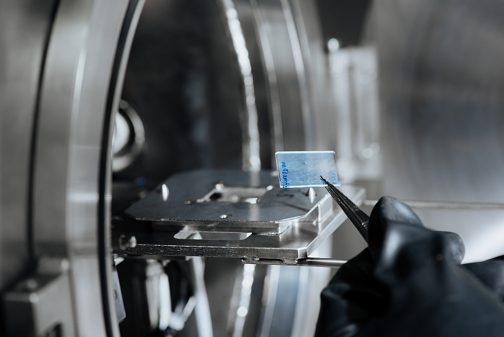
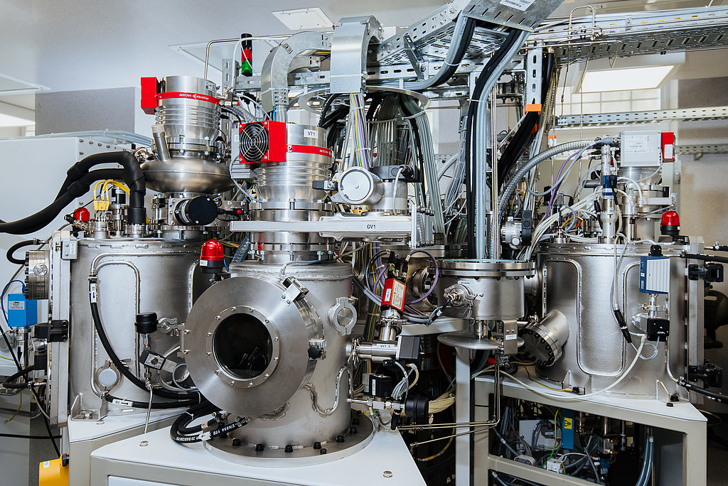
THIN FILMS LABORATORY has been established in 2017 to enhance the institute (ISSP) focus on thin films science and technology. The Laboratory provides thin film deposition service of a wide variety of inorganic materials, using different deposition techniques from existing and new tools, including the PVD vacuum multifunctional R&D cluster SAF25/50, the magnetron sputtering G500M cluster including High Power Impulse Magnetron Sputtering (HiPIMS), as well as PLD, MOCVD and ALD. The deposition tools are operated by highly skilled staff, enabling the deposition of novel materials as required by internal projects and external customers.
The TFL laboratory collaboarates with the largest vacuum technology industry among the Baltic countries: SIDRABE VACUUM, Ltd., SCHAEFFLER BALTIC, Ltd., GROGLASS, Ltd., ALFA, Inc.. The thin film deposition techniques developed at ISSP during the recent years are extensively used for thin film deposition in the framework of EU projects: H2020 CO2EXIDE, EUROFUSION, FP7 and EU Latvia (ERDF) projects as well as Competence centre BKC.
| Scientific degree | Name Surname | Position | Contact information |
|---|---|---|---|
| Dr.habil.phys. | Juris Purāns | Head of the laboratory and Leading researcher | Purans 67251691 |
| Ph.D. | Edgars Butanovs | Leading researcher | Edgars.Butanovs 67187511 |
| Dr.phys. | Lauris Dimitročenko | Leading researcher | Lauris.Dimitrocenko 67187479 |
| Dr.phys. | Boriss Poļakovs | Leading researcher | Boriss.Polakovs 67187511 |
| Dr.phys. | Mārtiņš Zubkins | Leading researcher | Martins.Zubkins 67251691 |
| Dr.phys. | Ilze Aulika | Leading researcher | Ilze.Aulika 25241686 |
| Dr. Habil. Phys. | Smagul Karazhanov | Leading researcher and Research Consultant | Smagul.Karazhanov |
| Dr.chem. | Tamara Tsebriienko | Researcher | Tamara.Tsebriienko |
| Dr.phys. | Andrejs Ogurcovs | Researcher | Andrejs.Ogurcovs |
| Mg. | Kārlis Kundziņš | Researcher | Karlis.Kundzins 67187875 |
| Mg.biol. | Viktors Vibornijs | Researcher | Viktors.Vibornijs |
| Esme Isik | Guest Researcher | Esme.Isik | |
| Anna Zajakina | Guest Researcher | Anna.Zajakina | |
| Mg. | Edvards Strods | Research Assistant | Edvards.Strods |
| Mg. | Luīze Dipāne | Research Assistant | Luize.Dipane |
| Jeļena Arhipova | Laboratory Assistant | Jelena.Arhipova | |
| Dr.phys. | Vera Skvorcova | Laboratory Assistant | Vera.Skvorcova 67187473 |
| Bc. | Emija Ļetko | Laboratory Assistant | Emija.Letko |
| Dr. | Ēriks Dipāns | Laboratory Assistant | Eriks.Dipans |
| Mg. | Aleksandrs Novikovs | Laboratory Assistant | Aleksandrs.Novikovs |
| Liora Kotļara | Laboratory Assistant | Liora.Kotlara | |
| Atabek Allaniyazov | Laboratory Assistant | Atabek.Allaniyazov | |
| Anna Zaiceva | Laboratory Assistant | Anna.Zaiceva | |
| Regnārs Ēriks Erdmanis-Hermanis | Laboratory Assistant | Regnars.Erdmanis | |
| Dāvis Cvetkovs | Laboratory Assistant | Davis.Cvetkovs | |
| Daniels Kaļiņins | Laboratory Assistant | Daniels.Kalinins | |
| Žanna Rudeviča | Laboratory Assistant | Zanna.Rudevica | |
| Dr.phys. | Aleksandrs Sazonovs | Technical Specialist | Aleksandrs.Sazonovs |
| Sven Oras | Project Manager | Sven.Oras | |
| Mg. | Dmitrijs Ščegoļevs | Project Support Specialist | Dmitrijs.Scegoļevs |
| Dr.biol., Bc.sc.soc. | Laura Žorža | Project Support Specialist | Laura.Zorza |
Thin Films Laboratory (TFL) has been established in 2017 to enhance ISSP’s UL focus on thin films science and technology. The methods of film deposition include evaporation (thermal, e-beam and pulsed laser deposition) and magnetron sputtering (DC, pulsed-DC, RF, HIPIMS) technologies. There is a number of deposition techniques integrated in a single multifunctional cluster tool developed and built by SIA "Sidrabe Vacuum ". Several stand-alone magnetron sputtering and evaporation units are in use as well.
The TFL laboratory strongly collaboarate with the largest vacuum technology industry (SIDRABE VACUUM, Ltd., SCHAEFFLER BALTIC, Ltd., GROGLASS, Ltd., ALFA, Inc.) among the Baltic countries. Thin film deposition techniques developed at ISSP UL during the recent years are extensively used for thin film deposition in the framework of the EU FP6 (X-TIP) and FP7 (EUROFusion CfP-WP15-ENR-01/UL-01) projects as well as Competence centre BKC. Apart from the standard versions of Magnetron sputtering, High Power Impulse Magnetron Sputtering (HIPIMS) processes are developed at ISSP UL using highly ionised pulse plasma source for sputtering and modification of material properties.
The Laboratory provides thin film deposition services of a wide variety of materials, using different techniques from existing and new deposition tools, including the multifunctional R&D cluster SAF50 plant, HIPIMS G500M, PLD, MOCVD and MOCVD. The deposition tools are operated by highly skilled staff, enabling the deposition of novel materials as required by internal projects and external customers.
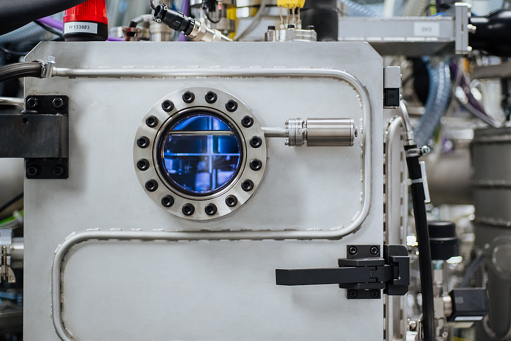
The SAF25/50 multifunctional R&D cluster plant (installed in a class 7-8 clean room) is well suited for research and development works as well as for feasibility studies and more general academic work in the field of thin film technologies. The plant is a multifunctional, expandable, modular and flexible system comprising an input/output chamber with ion gun, a central substrate transfer chamber with a radial telescopic transport arm, 7 deposition chambers and a glovebox. The plant is equipped with DC, pulsed-DC, RF, HIPIMS magnetron power supplies, e-beam gun, process control by Optical Emission Spectroscopy (OES), high pressure quadrupole gas analyzers and in-situ film characterisation by ellipsometry. Installation of two HIPIMS sources and a two channel Time resolved OES system for process control is currently underway. Capitalizing on HIPIMS advantages, this will open new venues for the development of thin film deposition methods for coatings of more complex composition and/or layer structure than obtainable with a single deposition source.
PLD will be installed and developed in the near future for production of thin films and heterostructures from various materials with complicated stoichiometry. PLD will allow a one-to-one transfer of elements from target to substrate, which is a strong advantage for the deposition of multiple element systems. Different atmospheres of deposition allow for varying of film properties in a wide range. One of the planned PLD applications is a sythesis of core-shell nanowire heterostructures, where core is a single crystal semiconducting material (e.g. ZnS, ZnO or GaN nanowire), and shell is layered VdW material belonging to TMDs materials group (e.g. MoS2, WS2, ReS2, etc.). Such heterostuctured materials are perspective for wide range of applications starting from sensors to photocatalitic water splitting.
A MOCVD reactor (Aixtron AIX-200RF) is available for the synthesis of thin films involving metals, liquid metal-organic compounds and gaseous non–metal chemical hydride and oxide gases. The Control of the rate of reactants flow is provided using thermostats for liquid metal-organic compounds, and carrier gas (N2, H2) flow. The control of non-metal chemical hydride gases flows involves both the carrier gas and precursor flows. The equipment will be renovated for the synthesis of classic LED structures, as well as for the synthesis of Ga2O3, ZnO-MgO, and group III nitride 1D nanostructures. There is a possibility to dope the materials, in order to obtain n- or p- conductivity. MOCVD equipment is used to manipulate chemical reactants creating different 1D, 2D, and hybrid structures.
Active projects:
Horizon Europe
Safer and More Reliable WBG/UWBG-Based MVDC Power Converters (SAFEPOWER) (2024-2028)
Smart Windows for Zero Energy Buildings (SWEB) (2023-2027)
Physical Cognition for Intelligent Control and Safe Human-Robot Interaction (Sestosenso) (2022-2025)
European Regional Development Fund
Latvian Council of Science
Innovative Thin Films of Rare-Earth Metal Oxyhydrides: Unlocking New Applications (2025-2027)
Novel metal hydride-based thin films for electronic and energy technologies (2023-2026)
Postdoctoral
European Space Agency Latvian National Programme
Accomplished projects:
Horizon 2020
CO2-based Electrosynthesis of ethylene oXIDE – CO2EXIDE (2018-2021)
COST
Highly Ionised Pulse Plasma Processes (2010-2013)
EC Frameworks Projects
EC 6. IP "X-TIP" Project (2004-2007)
European Regional Development Fund
Smart Metal Oxide Nanocoatings and HIPIMS Technology (2019-2022)
Nanowire photodetectors (2020)
Innovative glass coatings (2010-2013)
European Regional Development Fund (LIAA administrated)
Multilayer mirrored sapphire substrates for more efficient blue-white LEDs (2020)
Micromachined silicon substrates for the AFM, SEM and TEM nanomechanical tests (2018)
European Social Fund
Innovative materials for transparent electronics and photonics (2013-2015)
Nanomaterials for perspective energy efficient solutions (2009-2012)
EUROfusion
Latvia - France Program “OSMOZE”
NANOSTRUCTURED TEST SPECIMENS FOR COMBINED NEAR-FIELD MICROSCOPY (2012-2013)
Phthalocyanine architectures for sensor application (2012-2013)
Latvian Council of Science
Thin films of rare-earth oxy-hydrides for photochromic applications (2020-2021)
X-ray Absorption studies of metal hydrides under extreme pressure (XA-EXTREM) (2018-2020)
XAFS studies of local structure of functional materials with femtometer accuracy (2013-2016)
Structure in nanoxide compounds and self-organization in stochastic media (2009-2012)
National Research Program
Postdoctoral
Portable diagnostic device based on a biosensor array of 2D material sensing elements (2021-2023)
Dr. phys. Boris Polyakov, one of the leading researchers of Thin Films Laboratory, was elected as a corresponding member of the Academy on November 21, 2024.
The Latvian Academy of Sciences has concluded the evaluation of applications submitted for the competition for the most significant scientific achievements in Latvia in 2024.
In the section “Theoretical Science – Fundamental Research” in the field of theoretical physics, the research “Tomorrow’s Energy: Unlocking the Potential of Graphene, Batteries, Superconductivity and Photocatalysis” has been nominated as the most significant achievement of the year, the authors of which are LAS Academician Roberts Eglītis, LAS Academician Juris Purāns, LAS Corresponding Member Anatolijs Popovs from the Institute of Solid State Physics of the University of Latvia and Dr. Ran Jia from Jilin University in China.
Latvia:
- Sidrabe Vacuum, Ltd, www.sidrabe.com/.;
Sweden:
- Uppsala University (UU), Uppsala (Prof. Lars Österlund, Prof. Claes-Göran Granqvist);
Italy:
- Fondazione Bruno Kessler, (FBK), Trento;
- Istituto Nazionale di Fisica Nucleare – LABORATORI NAZIONALI DI FRASCATI , http://w3.lnf.infn.it/;
Polyakov, B.; Kadiwala, K.; Butanovs, E.; Dipane, L.; Trausa, A.; Bocharov, D.; Vlassov, S. Synthesis of ZnS/Al2O3/TaSe2 Core/Shell Nanowires Using Thin Ta Metal Film Precursor. ChemEngineering 2024, 8, 25. https://doi.org/10.3390/chemengineering8010025
Butanovs E., Zubkins M., Strods E., Vibornijs V., Kadiwala K., Ignatane L., Polyakov B., Vlassov S., Purans J. Impact of temperature and film thickness on α- and β- phase formation in Ga2O3 thin films grown on a-plane sapphire substrate. Thin Solid Films. 2024. 803. https://doi.org/10.1016/j.tsf.2024.140467.
Kadiwala, K.; Dipane, L.; Dipans, E.; Bundulis, A.; Zubkins, M.; Ogurcovs, A.; Gabrusenoks, J.; Bocharov, D.; Butanovs, E.; Polyakov, B. Synthesis and Investigation of ReSe2 Thin Films Obtained from Magnetron Sputtered Re and ReOx. Crystals 2024, 14, 690. https://doi.org/10.3390/cryst14080690
Zubkins M., Vibornijs V., Strods E., Butanovs E., Bikse L., Ottosson M., Hallén A., Gabrusenoks J., Purans J., Azens A. Deposition of Ga2O3 thin films by liquid metal target sputtering. Vacuum. 2023. 209. https://doi.org/10.1016/j.vacuum.2022.111789.
Zubkins M., Vibornijs V., Strods E., Aulika I., Zajakina A., Sarakovskis A., Kundzins K., Korotkaja K., Rudevica Z., Letko E., Purans J. A stability study of transparent conducting WO3/Cu/WO3 coatings with antimicrobial properties. Surfaces and Interfaces. 2023. 41. https://doi.org/10.1016/j.surfin.2023.103259.
Zubkins M., Strods E., Vibornijs V., Sarakovskis A., Nedzinskas R., Ignatans R., Butanovs E., Purans J., Azens A. Deposition and photoluminescence of zinc gallium oxide thin films with varied stoichiometry made by reactive magnetron co-sputtering. Journal of Alloys and Compounds. 2024. 976. https://doi.org/10.1016/j.jallcom.2023.173218.
Vibornijs, V.; Zubkins, M.; Strods, E.; Rudevica, Z.; Korotkaja, K.; Ogurcovs, A.; Kundzins, K.; Purans, J.; Zajakina, A. Analysis of Antibacterial and Antiviral Properties of ZnO and Cu Coatings Deposited by Magnetron Sputtering: Evaluation of Cell Viability and ROS Production. Coatings 2024, 14, 14. https://doi.org/10.3390/coatings14010014
Polyakov B., Novikovs A., Leimane M., Kadiwala K., Zubkins M., Butanovs E., Oras S., Damerchi E., Zadin V., Vlassov S. Comparison of the resistivities of nanostructured films made from silver, copper-silver and copper nanoparticle and nanowire suspensions. Thin Solid Films. 2023. 784. https://doi.org/10.1016/j.tsf.2023.140087.
A photochromic double layer coating with enhanced contrast and darkening speed. E.Strods, M.Zubkins, J.Purāns. LVP2024000039. 2024.
An antimicrobial multilayer thin-film materials coating. V. Skvorcova, M. Zubkins, J. Purans, V. Vibornijs, E. Strods, I. Aulika. EP4421207A1. 2025.
An optical tactile and pressure sensor. I. Aulika, K. Kundzins. LVP2024000016. 2025.
A method for deposition of yttrium monoxide film and yttrium monoxide coating. Halil Arslan. EP4033003A1.
Ierīce vakuuma pārklājumu izgatavošanai. J. Purāns, A. Āzens , M. Zubkins. 2024. LV15606.
A method for high power impulse magnetron sputtering deposition of rhenium oxide thin films. Zubkins Mārtiņš; Poļakovs Boriss; Šarakovskis Anatolijs; Purāns Juris. LV15743A