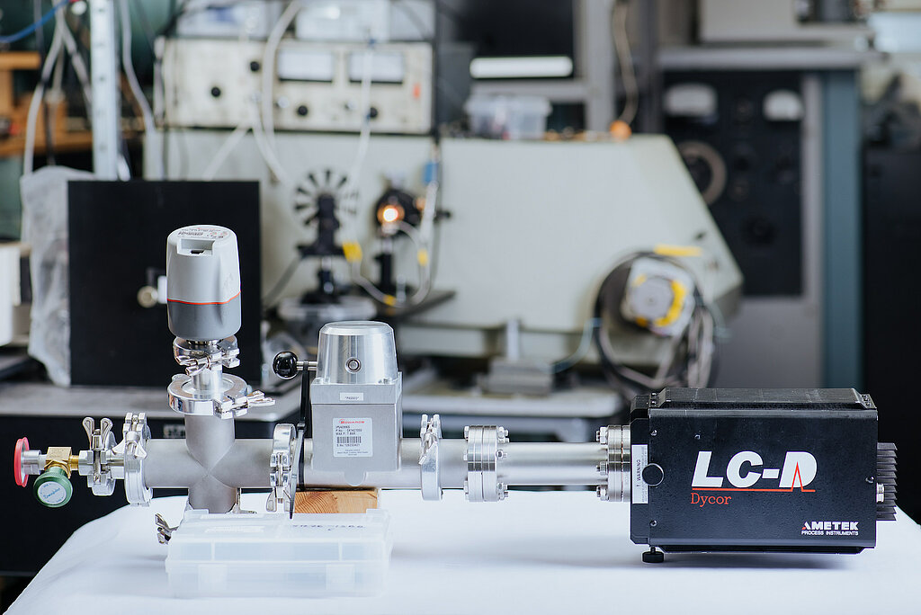
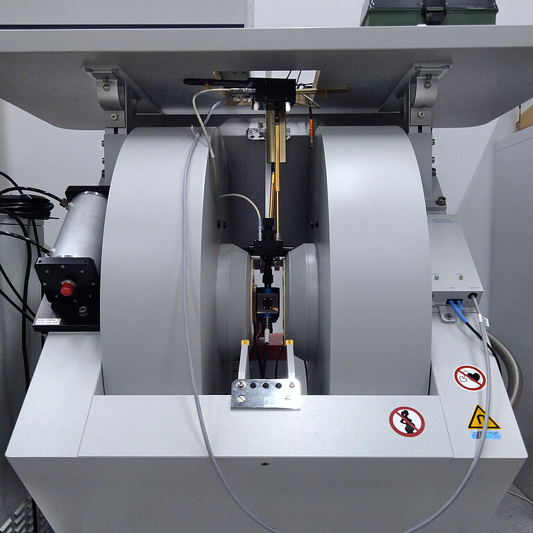
Portable Mass-Spectrometer
My name is Dycor LC-D Portable Mass-Spectrometer, but everyone just calls me Mass Spectrometer
Hello, friends! The smell of gingerbread is in the air, and I love it! Even though gingerbread is not a common Christmas snack where I come from. My roots are in USA, in the manufacturer of electronic instruments and electromechanical devices Ametek.
But I'll better tell you about myself. Officially, I am called Dycor LC-D Portable Mass-Spectrometer, but everyone just calls me Mass Spectrometer. Although my first ancestor, called a parabola spectrograph, turned 110 this year, we are carrying on a family tradition of determining the mass of different molecules in a sample very accurately. I would like to note here that we do not weigh the molecules, but determine the speed at which positively charged ions move through a vacuum chamber to a negatively charged plate. The speed at which each ion runs is determined by the weight of the molecule. So, I can tell scientists what a sample is made of, and I monitor and run diagnostics of processes to be sure all the samples are of good quality.
I am made of materials that make me compatible to work in the same team as the UHV or ultra-high vacuum systems, which I also monitor and make sure nothing leaks, because they are vacuum systems, in the end. My other responsibilities include monitoring of semiconductor and thin-film processes in the high vacuum range. By analyzing the sample, I can determine its purity, carry out adsorption and desorption measurements and chemical analysis.
Even though I look like an undistinguished piece of equipment in the picture, I have everything I need for high-quality work, wherever the scientists take me.
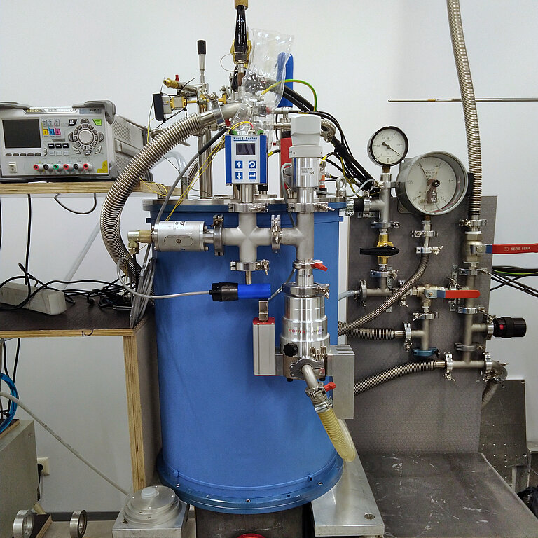
Optically detected magnetic resonance spectrometer (ODMR)
My heart - a magneto-optical cryostat
Allow me to introduce myself - I am an Optically Detected Magnetic Resonance Spectrometer, or as my friends call me - an ODMR Spectrometer. My heart, a magneto-optical cryostat, has arrived at the Institute of Solid State Physics, University of Latvia from the picturesque town of Abingdon in the United Kingdom, which, the experts say, is the oldest town in the whole of England. Due to its location, the town has been a meeting point for traders for thousands of years. Today, life in Abingdon is quieter and calmer, but it is home to the headquarters of Oxford Instruments. This leading manufacturer of high-tech equipment and services is also a place my magneto-optical cryostat comes from.
Although in the picture I look like a blue barrel with all sorts of wires and tubes, I am a very serious tool, and my main job at the Institute is the characterization of materials using the spectroscopy method and lasers. Basically, I am a whole system of different instruments that can be used to investigate in detail the mechanisms of luminescence and the origin of optical absorption bands using optically detected electron paramagnetic resonance (EPR).
Among my detection modes are photoluminescence, recombination luminescence, and magnetic circular dichroism. Specifications for my magneto-optical cryostat: magnetic field range is between 0 and 8 tesla; the microwave range is in the so-called Q, V and W frequency bands, which are 36, 65 and 93 gigahertz, respectively; the temperature range is from 1.5 to 300 kelvins; while the optical range - from 200 to 900 nanometers. I would like to add that the scientists use liquid helium while working with me. This is necessary to be able to trigger the cryostat's powerful superconducting magnet and to cool the sample to a temperature of 1.5 kelvin, which, it should be noted, is very close to absolute zero or −273.15 degrees on the Celsius scale.
More scientific information about me is here.
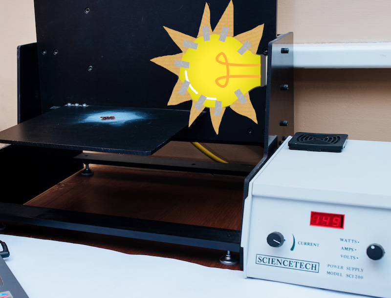
Solar Simulator
All we want is a little bit of sunshine
My name is Solar Simulator, and I was made in the Canadian company Sciencetech Inc., which has been designing and manufacturing optical instruments since 1985. We, Solar Simulators, are devices that provide illumination approximating natural sunlight or the solar spectrum. We are most commonly used in research areas such as photooxidation, photodegradation, photovoltaics, and photocatalysis.
I aim to provide a controllable indoor test facility under laboratory conditions to the scientists at the Institute of Solid State Physics, University of Latvia. The researchers can use my powers to test any photosensitive materials. I am a fully reflective Solar Simulator, and I can be used for UV applications by replacing my solar filters with UV filters. Sciencetech's proprietary Fully Reflective design allows the system to get far more UV power on target than equal size solar simulators of other manufacturers.
Now let’s talk about my technical specifications. As a light source for my work tasks, I use a xenon lamp with an AM1.5G filter corresponding to ASTM E927-05(2005) and IEC-904-9 standards. The spectral range of the lamp is from 250 – 2500 nm wavelength, illumination intensity - 100 mW/cm2. I can illuminate a 5x5 cm sample with a 7.6 cm diameter spot as long as it is 61 cm away.
At the institute, I mostly help work with researchers from laboratory of organic materials when they study photovoltaic cells for electric energy generation.
Find more scientific information about me here.
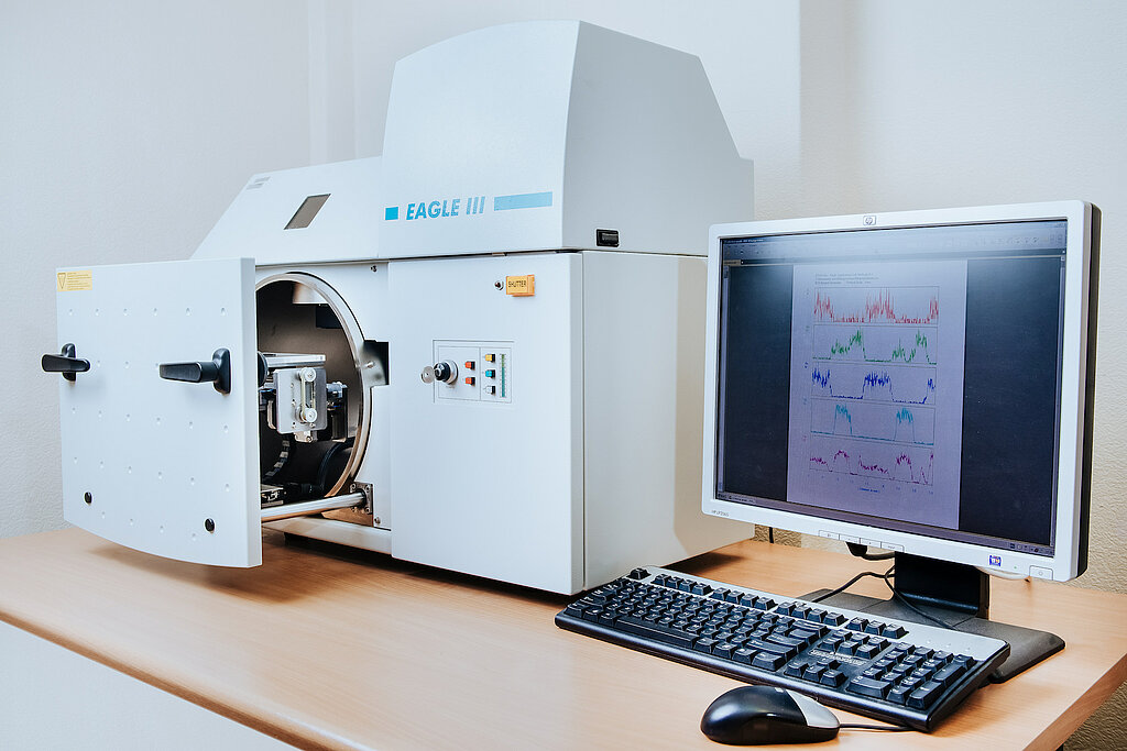
X-ray fluorescence analyzer
Endowed with an x-ray vision
Hi! My name is X-ray Fluorescence Analyzer, or as it says on my passport, XRF Eagle III XPL, and today I will tell you about myself and my superpowers. I come from Mahwah, New Jersey, USA, which is about 50 km from New York. Life in Mahwah is peaceful, with the Ramapo River and the Ramapo Mountains, mountain and valley reservations and parks. The town attracts residents of the nearby big city with its peace and beautiful nature. I have heard that in Latvia Sigulda is similar to my hometown due to its geographical location and natural views.
I work in the Laboratory of Optical Materials at the Institute of Solid State Physics, University of Latvia. I am a piece of equipment that characterizes materials, that is, I do the express analysis of the elemental composition of various materials and devices. Unlike other equipment units, I do not need special preparation of samples. I can analyze both the basic components and trace impurities in the sample. I am suitable for detecting the X-ray fluorescence (XRF) of chemical elements ranging from sodium (Na) to uranium. I do the sample excitation by X-rays focused on a polycapillary fiber lens with a minimum spot size of 50 microns. However, my X-ray vision has certain limitations, due to which I cannot detect elements lighter than Na.
I have a large sample chamber with a computer-controlled translation stage and can take my measurements both in air and vacuum (in the case of light elements). My arsenal also includes features such as a set of filters in the primary X-ray beam and variable focusing spot size. Also, depending on the element of interest and the composition of a sample, my eye can reach a sensitivity of up to 100 ppm! When I have done my work, I send linear 1D and 2D element distribution maps to the computer so that the scientists could work with them.
Full description is available here.
Differential scanning calorimeter and thermogravimeter
#TwoInOne
Hey, this week’s story is about me – the two-in-one - Differential Scanning Calorimeter and Thermogravimeter. If you’re looking at the picture right now, it’s hard to tell where I am. At first glance, I appear to be some computer. But take a closer look – there, on the left side with a red hat. Yes, that’s me! And my closest colleagues ARE computers. So, I am an equipment tool that characterizes materials using thermal analysis. I came to my new home at the Institute of Solid State Physics, University of Latvia straight from Caluire-et-Cuire, a Lyon suburb in France, located between two rivers - the Saône and the Rhône. I'm glad that now my work is situated on the very bank of the Daugava River, which is as wide as the Saône and the Rhône together!
At the Institute, I'm the guy who helps researchers determine how the properties of materials change under the influence of temperature. Depending on the sensor, I can analyze samples from room conditions up to 800°C and even 1600°C, and my temperature accuracy is ± 1°C! To heat up quickly and cool down a little slower is just child’s play. I can heat up at 100°C/min and cool down from 1600°C to 50°C in just 32 minutes.
Scientists use my abilities to learn the thermal behavior of materials exposed to extreme temperatures during production, service, or recycling. I help researchers determine the sintering temperatures of metal powders, the transition temperature of the glasses, and the crystallization temperature of composite in composite materials such as glass ceramics and other thermal characteristics of all sorts of organic and inorganic materials.
Detailed information about me is here.
UV/Ozone Cleaner
Like tanning booth but for materials
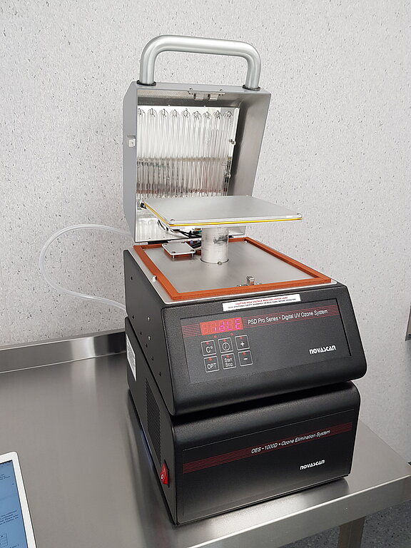
Hello! I'm a regular guy from the small town of Boone, Iowa, USA, which was founded less than 200 years ago thanks to coal mining and railroad development. In the heyday, coal mines and railroad traffic provided the city's residents with a living. A long time has passed since those days, but even today you can enjoy a 90-minute steam locomotive ride (and more) and feast your eyes on the picturesque views of the valley.
Even though I really liked my life there, I am happy that I can fulfill myself professionally in the cleanrooms of the Institute of Solid State Physics, University of Latvia (ISSP UL). I am one of the equipment units scientists use to synthesize and treat materials. I help ISSP UL scientists to remove contamination on the surface of samples. Using a high-power UV light source, I can create ozone, breaking surface contaminants into volatile compounds. These volatile compounds evaporate from the surface without leaving a trace and, look, everything is clean!
My kit includes a height adjustable sample stage or sample holder, I am equipped with an automated ozone elimination module. My stage can be heated up to 150°C, and I also have a high-intensity low-pressure mercury vapor discharge lamp. I might look plain, but I am indispensable.
Full equipment description here.
Ultrasonic cleaning unit
What's my purpose? Ultrasonics.
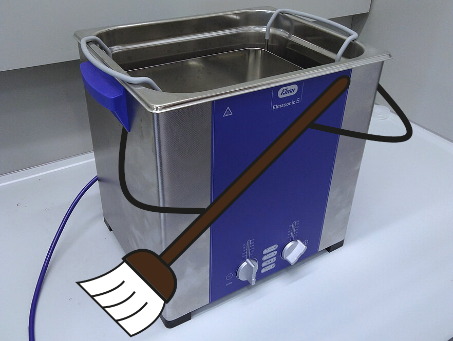
Good afternoon! My name is Ultrasonic Cleaner. My hometown is Zingen, located in the picturesque state of Baden-Württemberg in southern Germany. Now, I am perfectly settled in the cleanrooms of the Institute of Solid State Physics, but sometimes I miss the landscape of my native place, particularly the white peaks of the Alps...
I belong to chemistry laboratory equipment and am used in material synthesis and treatment. My superpower is ultrasound. Although my main function is cleaning, I am also useful for other purposes. One of them is the dispersion of small particles in solutions because such small-sized particles tend to "stick together" and form larger composite particles, which is often undesirable, for example, in various nanosolutions (in which the particle size is a few tens or hundreds of nanometers).
Sometimes I help in dissolving hardly dissolvable substances. For a mechanical stirrer such a task could take days, but, equipped with ultrasonic and heating functions (as higher temperatures increase the solubility of solids) I can perform such a task much faster.
Anyway, my main function - cleaning - is quite important. Often, there are cases when for various reasons a container or a part cannot or should not be cleaned with mechanical or chemical means. Here is where I come in and clean everything gently, environmentally friendly, and quickly. In addition, I save manual labor for the laboratory staff. I am particularly good at cleaning various fine and delicate parts.
Find out more about me here.
X-ray Diffractometer (XRD)
Expert at material characterization
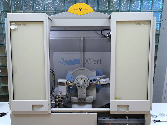
My name is X-ray Diffractometer, and I come to the ISSP UL from the British town of Malvern, which is famous for its natural mineral water springs. And now you will learn that the town is also known among researchers because it is the hometown of the Malvern PANalytical – a company that manufactures scientific instruments.
I help the ISSP UL scientists in their materials research – I reveal the crystalline structure of materials. The method I use to obtain this information is the only one that provides structural information about the test sample - chemical composition, crystal structure, crystallite size, strain, and layer thickness. Therefore, the researchers use my powers to analyze a wide range of materials, from powder X-ray diffraction (XRPD) to solids, thin films, and nanomaterials. I can be used for high-resolution powder diffraction, phase identification and quantitative phase analysis, analysis of thin films and coatings, crystallite size and strain determination, and kinetic and non-ambient experiments.
My chief task is to help scientists obtain the highest quality diffraction data so that they can characterize a wide range of materials. In addition, I am easy to use and can quickly switch between different tasks. I alone can tell scientists about the sample being analyzed in great detail. I usually work with the researchers from the Laboratory of Ferroelectric Materials and Laboratory of Optical Materials. I remember once I had quite a task: analyze the shift of atoms under the influence of temperature and electric field with the resolution of a few picometers in perovskite materials.
Detailed information about me is here.
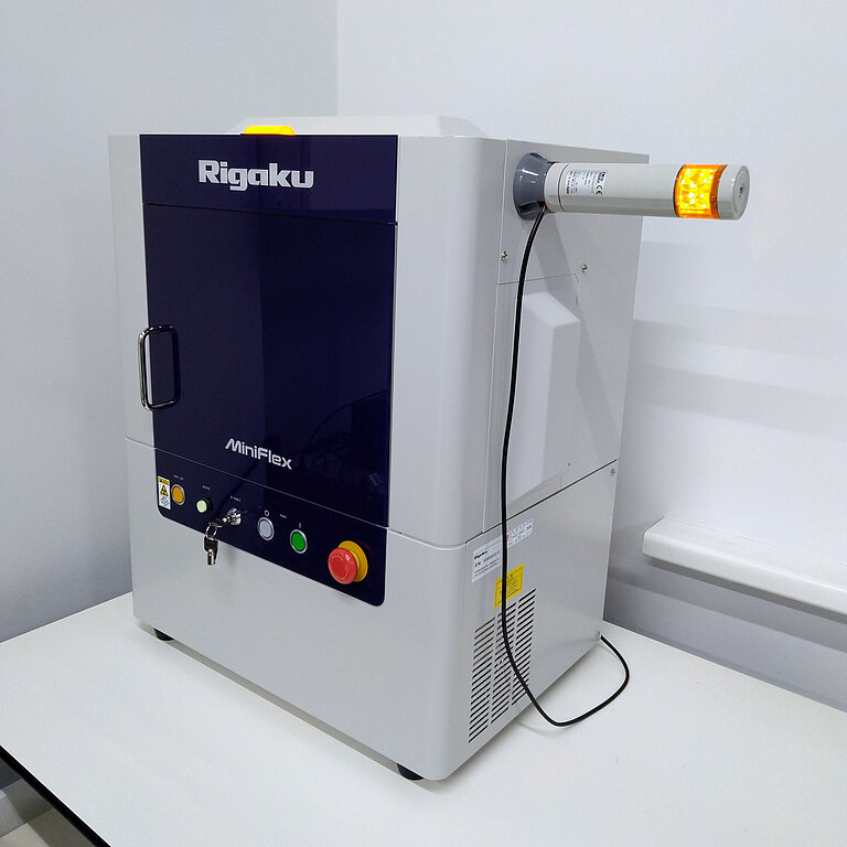
X-ray Diffractometer MiniFlex
I'm flex'ing
Konnichiwa! My name is X-ray Diffractometer MiniFlex or as my friends call me - MiniFlex. I was born in Rigaku - an international scientific instruments manufacturing corporation and have travelled to the Institute of Solid State Physics, University of Latvia (ISSP UL) from Japan. Most probably everyone has an idea of my land – for somebody, it is a land of the fearless samurai, for somebody else - the flowering Sakuras or sushi, yet someone thinks of Japan as the land of super-agers. I would be glad if after reading my story, Japan would associate with me, just a tiny bit.
Let’s get to it then, shall we? I am a multifunctional piece of equipment, and I can qualitatively and quantitatively analyze polycrystalline materials or describe their atomic structure. As most solids have a polycrystalline structure, I can analyze all the materials around us, both natural and artificial. I consider my compact size an advantage and I can offer fast measurements while ensuring high enough quality for further analysis.
I am a benchtop X-ray diffractometer and I can be used for phase identification and quantification, crystallinity (%) evaluation, crystallite size and strain, lattice parameter refinement, Rietveld analysis, and molecular structure determination. I can carry out measurements on powder samples as well as on larger objects with a minimal size of ≈ 1 cm2 and a plane surface. If the sample happens to be bigger, it is possible to cut and polish it. Together with me, the ISSP UL scientists obtained an extensive database that combines more than 426 thousand entries and the world's largest sources of inorganic diffraction data.
Detailed information about me is here.
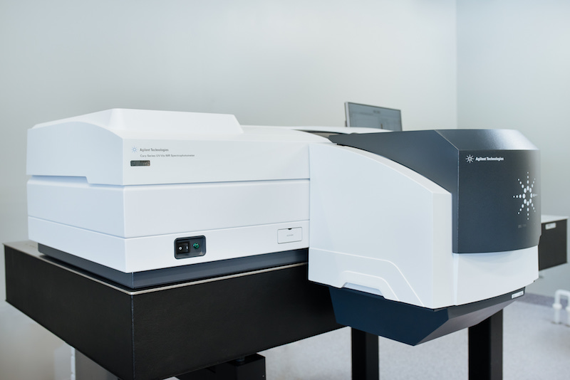
Spectrophotometer
I have superpowers.
Hi! I am a Spectrophotometer, and I come from a land far, far away. My hometown is Santa Clara, California, located at the heart of Silicon Valley. Yes, I was created in a place globally known as the center of high technology and innovation.
As you can see, my name is long and quite descriptive - it gives a sense of what I can do. My main superpowers are speed and accuracy: I can collect hundreds of UV-Vis-NIR spectra overnight or characterize optical components or thin films in minutes. Ok, ok, sometimes, if the sample is complex, it can take a few hours. For other similar devices, such a task can take even several days!
With my help, the ISSP UL scientists can get a complete sample characterization. They just set up their method, collect a single baseline, insert one or sometimes more samples, and walk away. I do everything automatically, allowing them to gain insight into advanced materials with unprecedented photometric accuracy - 10 Abs.
I am a turn-key solution for research, development, and quality control when working with optics, thin films and coatings. My multiangle specular reflectance and transmittance capabilities allow my colleagues, the scientists, and their industrial partners to design experiments that they could only dream about…
Detailed information about me is here.
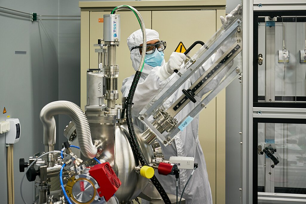
Pulsed Laser Deposition or PLD System
A piece of equipment that helps scientists not only deposit thin films but also study them at the atomic level.
Spring is finally here in Latvia and I long for my homeland a little bit because all the gardens, parks and fields are filled with blooming tulips, like every spring. Yes, yes, you guessed it right - I am Dutch! But I am not too sad to miss all the tulips because I have an exciting job in the Institute’s cleanrooms.
My name tells you what I do. I use a pulsed laser to deposit thin films on a variety of materials. I am a state-of-the-art equipment unit for the study of thin films at the atomic level available. Moreover, I am ideal for the research of many varied materials, including composite oxide materials.
How do I work? Pulsed Laser Deposition systems typically use a focused pulsed excimer laser to vaporize a small amount of a solid target material in a vacuum chamber to produce a thin film with the same chemical composition as the original target material. The PLD process enables the deposition of many complex materials at different substrate temperatures and over a wide range of background gas compositions and pressures.
Most often, I work with scientists from the Laboratory of Thin Films. I am delighted when I may be helpful to young scientists. I am currently working on a postdoctoral project to develop a portable diagnostic device based on a biosensor array of 2D material sensing elements. It is these 2D elements that I help to make.
Detailed information about me is here.
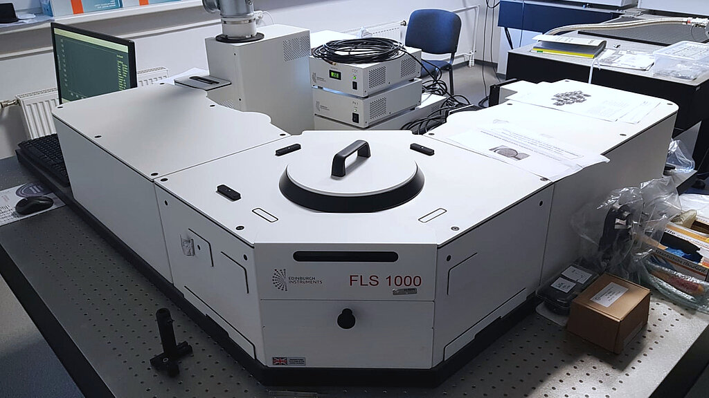
Photoluminescence Spectrometer
I have come a long way from my native Scotland to live and work in the Laboratory of Spectroscopy, Institute of Solid State Physics, University of Latvia.
Let me introduce myself - I am Sir Photoluminescence Spectrometer. I have come a long way from my native Scotland to live and work in the Laboratory of Spectroscopy, Institute of Solid State Physics, University of Latvia. My main duty is to characterize the optical properties of materials using excitation sources, monochromators, detectors, and optics. I have a big heart, so I use my whole arsenal of tools to characterize the materials. I am double-accurate because I have two monochromators in each hand, allowing me to get more accurate measurements than other laboratory equipment units.
I help scientists to get to know different noble families - solid and liquid samples, powders and thin films, and organic and inorganic materials. I make them shine brightly, and I can quickly get emission and excitation spectra. In, out, next! This is my philosophy of life. Leave the tiresome lens height adjustment with a ruler to my brothers in other laboratories. I am ready to serve right away! I can also measure maps of spectral emission in which the brightest luminescence bands fly like islands in the dark ocean. In the integrating sphere with a white interior, I determine the luminescence efficiency of the material, and I also have skills in measuring absorption and reflection spectra.
My work is appreciated by representatives from the Laboratory of Spectroscopy and the Laboratory of Organic Materials, who are happy to measure luminescence decay kinetics using a UV laser. I am versatile, but I like to keep my secrets. Guess what? You will never know what I have on my sample holder until you take off my lid and see.
Detailed information about me here.
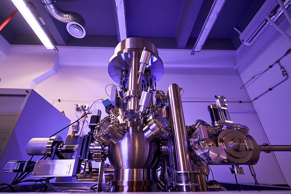
Electron paramagnetic resonance (EPR) spectrometer
Guten Tag, meine Damen und Herren! Today is my turn to tell you about myself - an accurate and reliable EPR spectrometer from the German company Bruker, whose main task is to characterize radiation defects in solids.
My name is EPR spectrometer. In my passport, I have a long and complicated name - Bruker ELEXSYS-II E500 CW-EPR. My purpose and vocation - to characterize radiation defects using the electron paramagnetic resonance method, which is a non-destructive spectroscopic method for the identification and analysis of paramagnetic species in solids. I do my job with the precision typical of Germans. Yes, yes, I am from Karlsruhe, Germany. It is the city where one of the best technical universities in Europe is located - the Karlsruhe Institute of Technology where, in turn, the origins of the Bruker company are found.
In general, my services are in demand by chemists, material scientists, physicists, and biologists. At the Institute of Solid State Physics, University of Latvia, I work with researchers from various laboratories, but most often, I cooperate with scientists from the Laboratory of Spectroscopy. They rely on my characterization skills to obtain information about transition metals, rare earth elements, as well as the properties and purity of different materials.
The most ambitious and famous project I have been involved in is EUROfusion. For the purposes of this project, I have helped ISSP UL scientists study the formation and transformation of defects in radiation-resistant materials that could be used in fusion reactors. Let me remind you that EUROfusion is a joint effort of 29 countries to develop fusion as an efficient form of electricity generation.
Detailed information about me here.
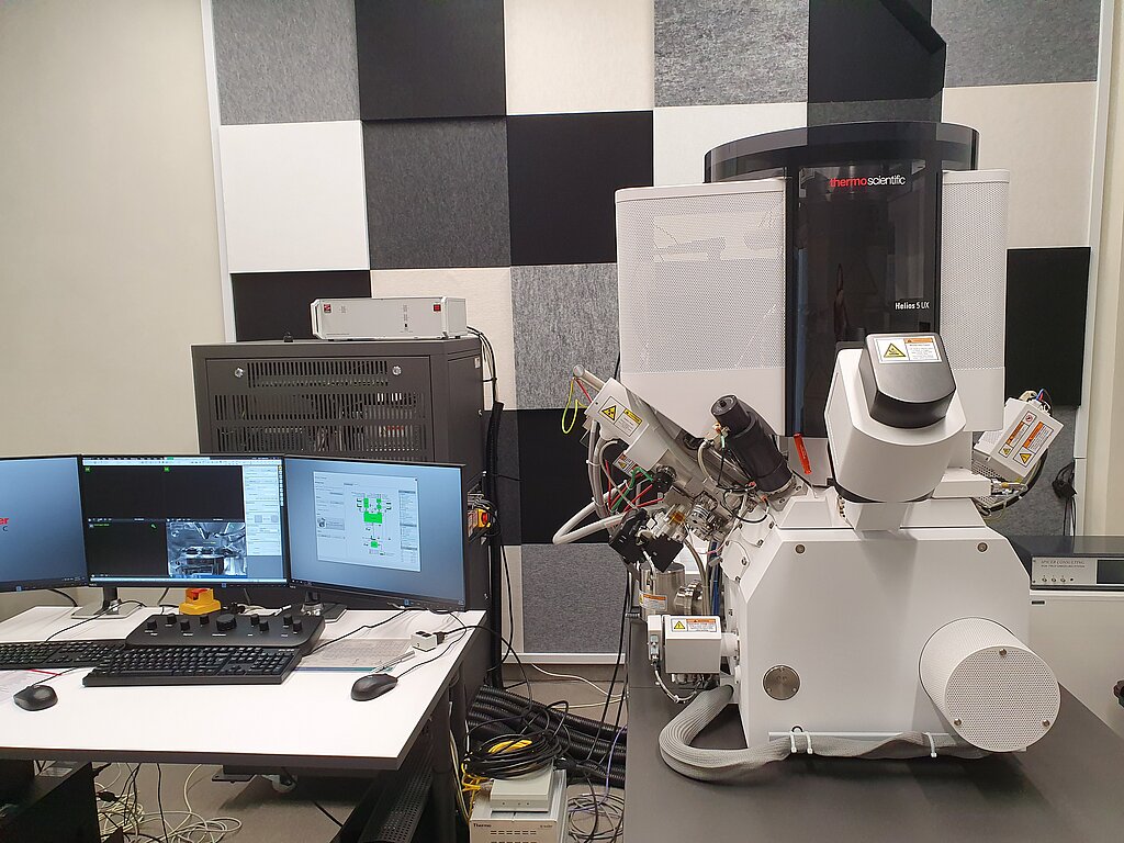
SEM Helios
This week our equipment story is about the Scanning Electron Microscope – SEM Helios 5 UX – the only one of this kind in the Baltic Sea region.
My full name according to my passport is SEM Helios 5 UX or simply SEM Helios, the scanning electron microscope. I come from the Netherlands and now reside at the Institute of Solid State Physics, University of Latvia. Without hesitation, I can claim that currently, I am the best microscope of my kind in the whole Baltic Sea region.
My task is to characterize materials. My uniqueness is that I can show scientists the analyzed samples in high image resolution, which in turn reveals the structural details of the samples, nanoparticle size distribution, and morphology. Thanks to the electron detectors, I provide extensive information about material samples by imaging. My energy dispersion detector is used for the chemical microanalysis of samples, while the electron backscatter diffraction detector allows quantitative analysis of microstructures. And that's not all! With a focused ion beam, I can get inside the material and study it in a volume of over tens of microns while reconstructing a sample in 3D visualization. By the way, I am also quite independent - when I get instructions, I can cut out tiny plates from large samples during the night so my very energetic brother, the transmission electron microscope, can look at them in the morning.
I usually work with scientists from the Laboratory of Microscopy, but my attentive eye is used by many, both from ISSP UL and other institutions. I am very proud of my input in the development of doctoral dissertations for the next generation of researchers - this is my contribution to the future. I can also add that the material sample images I have created are also seen by a wider audience – for example, in the ISSP UL’s calendars. In general, I am fortunate to have a job I love and do well!
Detailed information about me here.
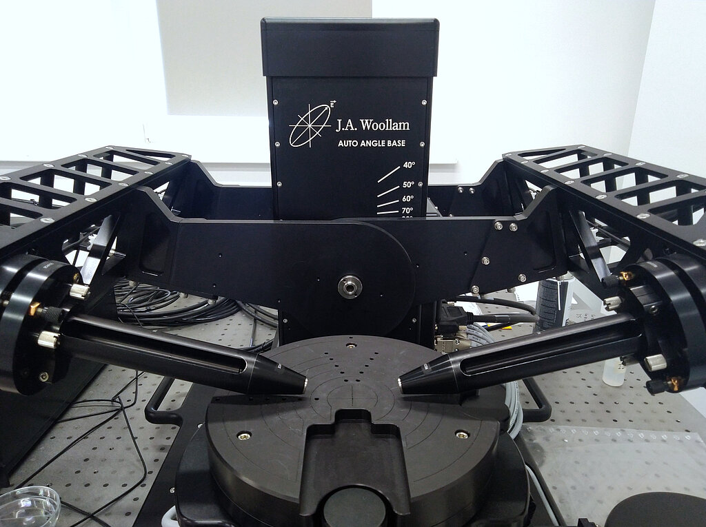
Spectroscopic Ellipsometer
I'm a Spectroscopic Ellipsometer - a simple guy from Lincoln, Nebraska, USA, and I bring a more global vibe to the series of equipment stories.
I'm a Spectroscopic Ellipsometer - a simple guy from Lincoln, Nebraska, USA, and I bring a more global vibe to the series of equipment stories.
After a long journey, I live in the Laboratory of Spectroscopy, ISSP UL. I am not such a wide-range expert as my colleagues, who can apply coatings, process samples, and tell the composition. However, I am precise, accurate, and universal.
My task is to irradiate the sample with a xenon lamp and measure the change in polarization of the reflected light. Analyzing this information, I can determine the thickness and optical constants of the thin film and, with the help of this data, characterize its composition, roughness, and impurities. See, I can do a lot! I can measure most material types: dielectrics, semiconductors, metals, superconductors, organic materials, biological films, and composites.
So far, my most interesting work has been on a project aimed at developing a microfluidic system that will improve the diagnosis and effectiveness of treatment for prostate cancer by performing a simple, fast, and inexpensive blood or urine test. My best friends are scientists from the Laboratory of Spectroscopy and Laboratory of Micro and Nanodevices. I’m sure I still have a lot of interesting tasks ahead of me.
Detailed information about me here.

Battery Test Station
The functional and the charming - Battery Test Station, which helps our scientists to develop new materials for battery production.
After two gentlemen, I finally have the opportunity to tell you about myself. I believe that gender equality also applies to telling stories. I am French, born in Grenoble at the foot of the Alps. I may not look as impressive as my colleagues from previous stories, but I am delicate, elegant, and just as important and functional. Officially, my name is Multi-channel Potentiostat/Galvanostat, but I prefer to be called Battery Test Station.
My work is related to material characterization and I am particularly good at battery testing due to the current range and high precision. Like any woman, I am great at multitasking. There are 15 independent measurement channels in my wardrobe (my little black dresses from Coco Chanel) that allow scientists to take multiple parallel measurements. One of them is specifically designed for measuring very low electric currents in the range of one nanompere. I am tireless and able to work for long periods of time, which is essential when I characterize the battery lifetime. I help scientists develop new battery materials so that those materials could be used to manufacture new and improved batteries. My possibilities are not limited to batteries - I can describe all kinds of electrical and electrochemical systems. My speciality is battery testing because of my accuracy and the wide range of electric current.
Detailed information about me here.
X-ray Photoelectron Spectrometer (XPS)
Contrary to the Multifunctional Cluster, introduced to you last week, I am a foreigner. I am a British gentleman and have covered quite an interesting way to get to the Spectroscopy Laboratory of the Institute of Solid State Physics, University of Latvia.
Contrary to the Multifunctional Cluster, introduced to you last week, I am a foreigner. I am a British gentleman and have covered quite an interesting way to get to the Spectroscopy Laboratory of the Institute of Solid State Physics, University of Latvia.
My job is to analyse materials by spectroscopic methods. Since I have exceptionally good eyesight (high-efficiency lenses and detectors), to analyse a sample of any material and tell all about its composition is a child’s play for me. Just like my fellow countryman Sherlock Holmes (I have a posher hat, by the way!), who could tell the smallest details about the crime scene by just looking at it, I can tell a lot by just throwing my X-ray eye at the surface of a sample: where it comes from, what coating it has, and whether it is a metallic or oxidized coating. All this information I get from the surface of the sample – the depth of a few dozen atomic layers. However, if you are interested in the composition of the sample in volume, my friend Dr Watson, an argon ion gun that can quickly clear the way to deeper layers, is at my disposal. An hour is usually enough for me to provide information about the sample and its composition. However, sometimes a sample must stay under my close supervision even for a day or longer to thoroughly analyse each element and each layer in its structure.
Many laboratories at the Institute seek my help, yet my skills are especially appreciated by scientists from the Laboratory of Thin Films. I often help companies that are interested in sample composition and structure. I am open to cooperation, and I am particularly pleased to provide my services in the investigation of some interesting cases. If you have a tricky case or a case that seems to lack a solution – I'm at your disposal!
Detailed information about me here.

Multifunctional Cluster
Hello! My name is Multifunctional Cluster, although I would rather say I am a Multi-Artist. I currently reside in the cleanroom facilities of the Institute of Solid State Physics, University of Latvia. I was born nearby - in the high-tech company Sidrabe. In fact, I am the result of a collaboration between science and industry. A Multi-artist because I combine 7 different modules, but it is possible to add some more.
My job is to pre-treat samples, sometimes I use an ion gun to do that. My speciality is thin films. I can apply various materials’ thin films by different methods in different thicknesses and as many layers as needed. And by saying thin I mean nanometers, which are at least a million times smaller than a meter. I take the sample through the modules so that it does not come into contact with the circumambient air and doesn’t get dirty. I assist scientists both in research and in various innovation projects related to, for example, sensors. I have a special power too - I can apply organic thin films, which is especially important in creating various photonic and electronic devices, from OLEDs (organic light-emitting diodes) to OFETs (organic field-effect transistors). I keep a close watch on the things happening in the world and I am really proud to be able to help with research in the fight against the pandemic, because I can also apply special antiviral coatings, thus reducing the risk of getting sick!
Although electricity prices have skyrocketed and I have a very good appetite for electricity (mind you – I only look chubby and round!), I would love to get an extra module and meet new and enthusiastic researchers! See you soon!