ISSP UL's Thin Film Laboratory is working on the development of new functional materials and coatings. Our main research areas are: thin films, nanomaterials, nanocomposites, electronic and optoelectronic devices, biosensors, printable electronics. We are currently looking for additional forces for the research of 0D, 1D and 2D (nanocrystals, nanowires and layered graphene-like materials) materials.
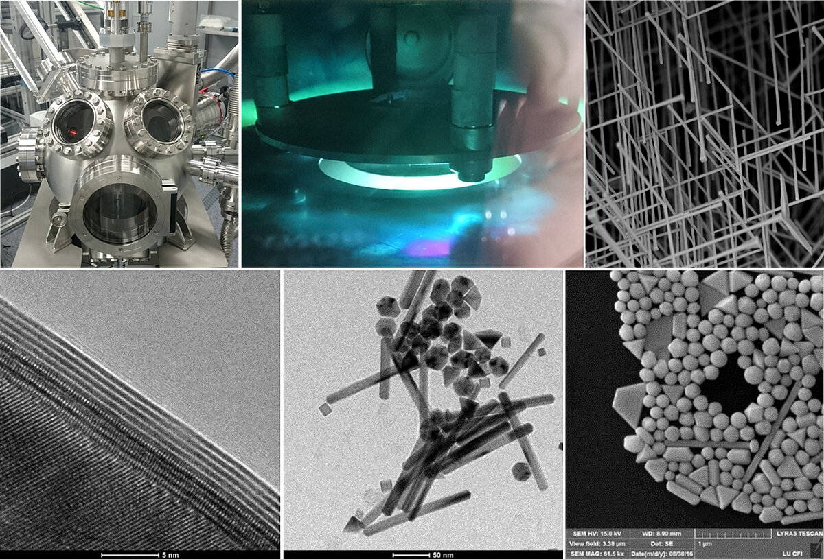
0D nanomaterials or nanoparticles are a cornerstone of nanotechnology. 0D nanomaterials have many potential applications in materials science, photovoltaic science, catalysis, energy, sensors, biomedicine and inkjet devices. Functional inks can be formed on the basis of nanoparticles. Functional inkjet printing is a promising new technology, inexpensive and environmentally friendly, and is creating a new paradigm in digital manufacturing where electronic devices and circuits can be printed on demand.
1D nanomaterials are nanowires, nanotubes, nanobelts, etc. Nanowires are ultra-fine wires with a typical diameter in the range of 1 to 100 nm and a large length to diameter ratio. Nanowires are now one of the most important objects in modern science and have promising applications in nanotechnology, including high-density data storage, electronic and optoelectronic nanodevices, energy applications (supercapacitors), nanoelectromechanical devices (NEMS) and others.
2D layered materials (such as graphene), due to their unique structure (strong bonds in the layer and weak interaction between the layers) and the promising physical properties that appear when the thickness of the material is reduced to a single atomic layer, today are considered to be very prospective for a wide range of applications, including electronics, optoelectronics and photonics, energy and sensors. A particularly interesting and promising application is the use of 2D materials in flexible electronics, which is considered to be potentially ubiquitous in future devices in everyday life.
Responsibilities
- Synthesis of 0D, 1D and 2D materials using different physical or chemical methods
- Characterization of 0D, 1D and 2D materials using morphology and structure research methods
- Inkjet printing of electrical and electroluminescent devices and biosensors
- Data processing, analysis and presentation
Depending on the student's previous experience and education, the emphasis may be on material characterization and physical properties (physics), materials synthesis (materials science, chemistry), electrical devices and biosensor inkjet printing (engineering).
Requirements
- Master's degree in physics, chemistry, materials science or engineering (if sufficient knowledge of physics or chemistry). May be a final year master's student.
- Willingness to enter doctoral studies and develop a doctoral thesis
- Basic knowledge of at least one of the following areas and a desire to master most of the others: synthesis of materials, methods of analysis of physical / chemical properties of materials, vacuum technologies, inkjet technologies, electronics and electrical measurements, computer control of equipment and optimization of industrial processes
- Good knowledge of English
- Personal competences: ability to work independently and responsibly, analytical and technical thinking, ability to work in a team, self-initiative
We offer work in a rapidly growing team in the field of high-tech at the leading Baltic materials research institute. Obtaining a doctoral degree confirms competence in this field of technology and significantly increases competitiveness in both the academic and industrial labour markets.
The position provides for a 50-100% load with a competitive salary, which depends on the candidate's previous experience. Remuneration may increase during the job, depending on the candidate's abilities and initiative.
Send the CV with copies of qualification documents (diplomas, transcripts) or additional questions to Boris Polyakov at boris@cfi.lu.lv or Edgars Butanovs to: edgarsb@cfi.lu.lv