More and more often in such devices like photovoltaic cells or light emitting diodes, the classical inorganic materials are being substituted by the organic materials. A huge variety of materials, a molecular design which allows to control and improve the properties of the material, as well as the possibility to manufacture devices using wet casting methods thus decreasing the cost, are advantages that make the organic materials an attractive field to the materials science. Such properties as light absorption, an electrical conductivity, charge carrier mobility, efficiency and wavelength of luminescence, will mainly determine the potential use of the material. The performance of the device will depend not only on the material itself but also on the compatibility between all the materials in the device. As the devices made of organic materials mostly consist of several layers (electron or hole transport layers, the electron or hole blocking layers, an active layer which consists of the mixture of two or more materials, electrodes), the compatibility of materials becomes especially significant. Most directly it is related to the energy levels of materials. Energy level alignment between different layers can diminish the losses in the device and improve its performance. This is the reason why easy and relatively simple methods for energy level and their changes determination are needed.
Ultraviolet photoelectron spectroscopy is the most often used method for energy level determination. However, it is an expensive and complicated method. Substitution with simpler yet less often used methods- photoelectron yield spectroscopy and scanning Kelvin probe- could be possible.
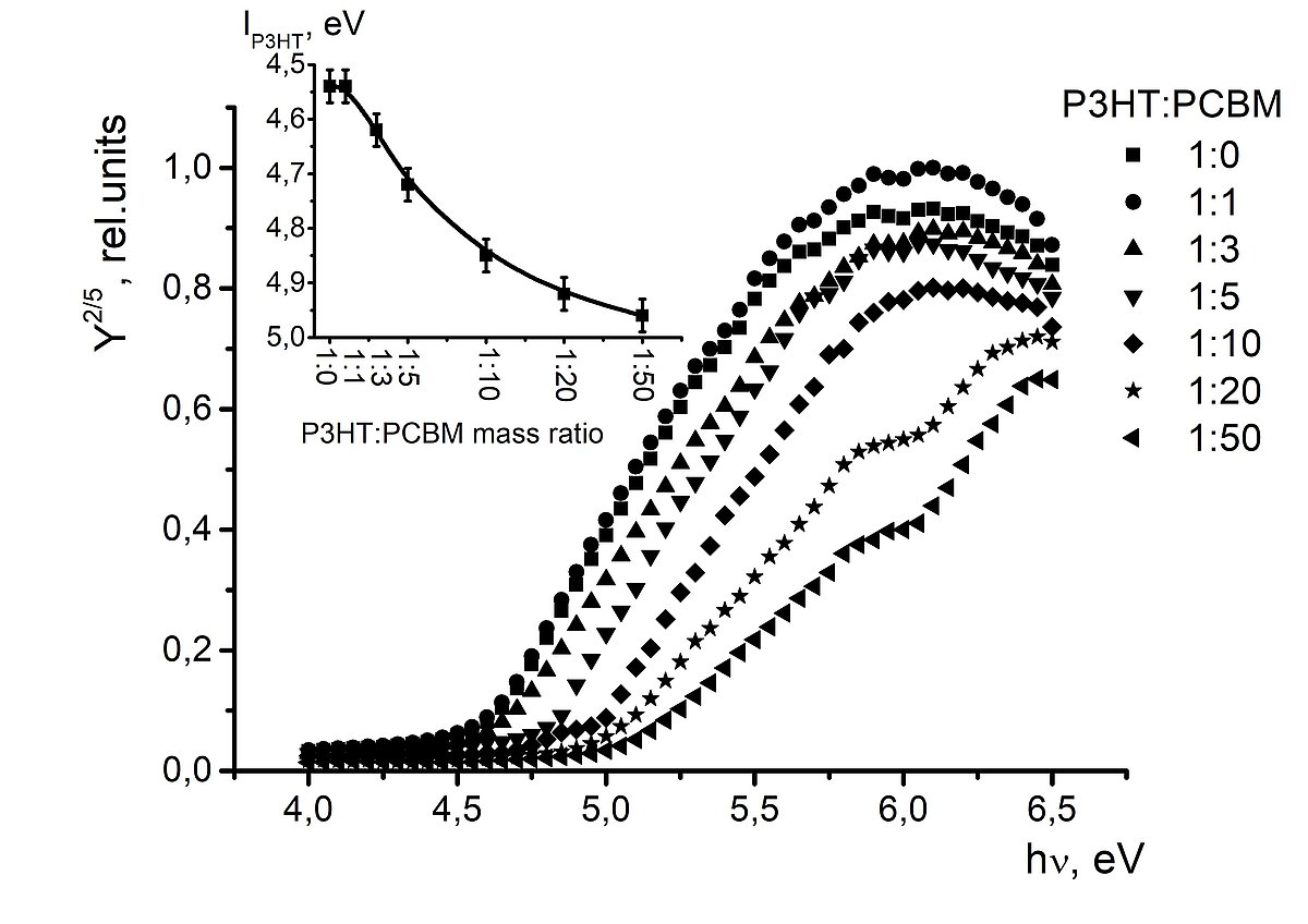
The experimental setup for molecule ionization energy determination using photoelectron yield spectroscopy was built. This method was used to determine the ionization energy of the materials, in the studies of the electrode-organic compound and the organic compound- organic compound interface. Organic compound- organic compound interface studies were made for classical planar structures, as well as for bulk heterojunction systems, which to the best of our knowledge has not been done yet. The results, as well as the conclusions about the advantages and disadvantages of such a method, are shown.
A surface potential using scanning Kelvin probe was obtained for various materials (metals, organic semiconductors, and organic dielectric materials). The obtained results show that the surface potential dependence on metal work function changes with the film thickness and the electrical conductivity of the material.