Microchips are the invisible scaffolding that envelops the modern world. With the ever-growing demand for faster, more efficient processing power, the semiconductor race has intensified across Europe. In this rapidly evolving landscape, Latvia aims to reposition itself from a technology consumer into a high-value developer.
In Latvia, the electronics and semiconductor-related sector already constitutes a substantial economic pillar, with an annual turnover exceeding €1.5 billion and employing nearly 8000 specialists.
However, the local industry stands at a turning point. Historically focused on system integration – assembling and programming devices using pre-existing chips – Latvia is now trying to bridge the gaps in chip prototyping, fabrication, and physical testing.
Jānis Sperga, a leading expert from the Latvian Microchip Competence Centre, recently highlighted the strategic shifts required for the region to thrive. For example, due to the microchip design cycle of 1-2 years, local innovators in fast-moving sectors like defence and telecommunications must look ahead and anticipate technology needs 3-4 years into the future.
He also notes how instead of trying to compete directly with massive Asian manufacturing hubs, European regions achieve the best results by securing specialized deep tech niches via novel research and discovery. This is where the Institute of Solid State Physics, University of Latvia (ISSP UL) is stepping in.
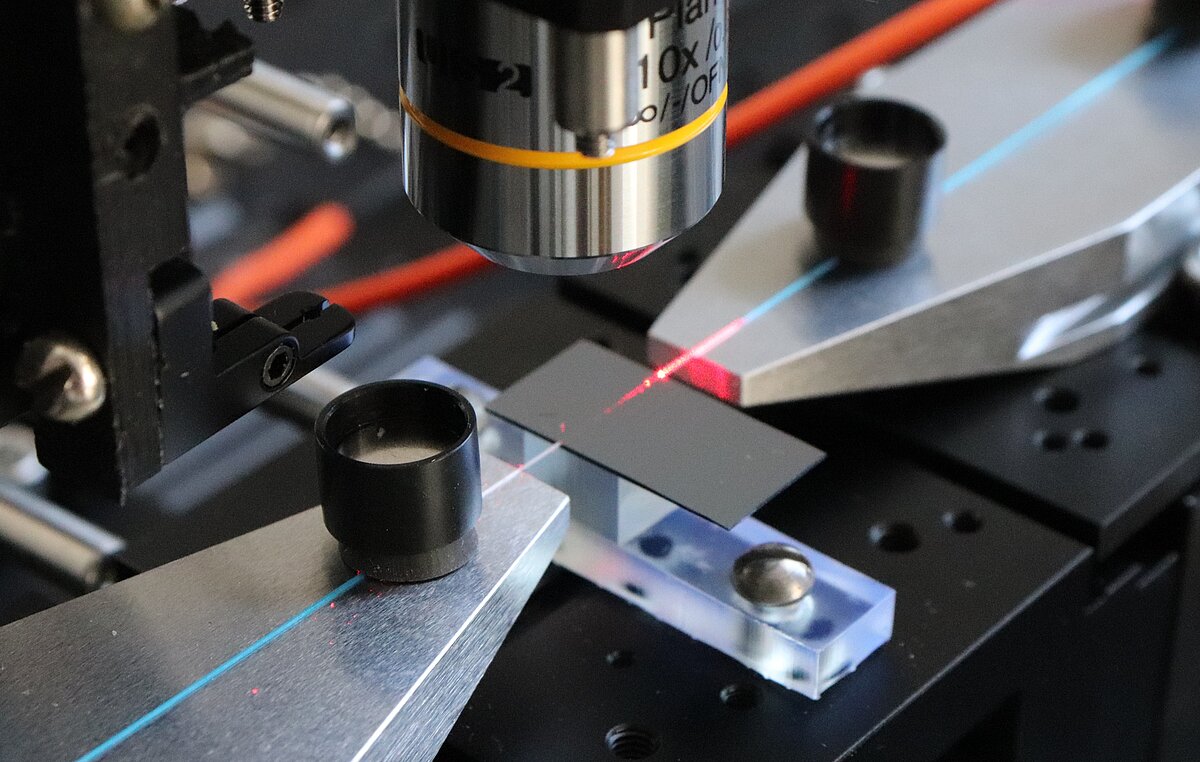
The institute is working towards an established Latvian presence in the microelectronics industry by moving from classical silicon microchips to the next frontier of hardware – photonic integrated circuits (PICs).
While traditional chips rely on electricity flowing through copper connections – a method plagued by data bottlenecks and power dissipation at extreme speeds – photonic chips guide light waves through microscopic channels. This allows data centres to interconnect high-performance computing blocks at unprecedented speeds with minimal energy losses.
It doesn’t end with just fundamental & applied research – ISSP UL actively tries to commercialise these innovations and foster the local economy. A prime example is the spin-off company AP4PIC, an institute-backed startup dedicated to advancing the assembly and packaging technologies required for PICs.
ISSP UL also utilises commercial avenues like the BioPhoT platform where the Phipic project is exploring the combining of inorganic materials (such as silicon nitride and indium phosphide) with polymers to achieve greater flexibility and functionality in photonic chips.
True semiconductor innovation requires elite global collaboration. That’s why ISSP UL maintains close institutional ties and cooperative projects with world-leading research institutions, for example, in Taiwan, the epicentre of global semiconductor manufacturing and design. This shortens the path from laboratory concept to scalable market innovation by letting Latvian researchers in on top-tier fabrication insights.
By continuously upgrading our research infrastructure, fostering international ecosystems, and translating complex physics into commercial deep tech enterprises, ISSP UL aims to establish Latvia as a meaningful centre of innovation that global partners can confidently collaborate with, invest in, and rely upon.