
On 9 February 2026 at the Institute of Solid State Physics, University of Latvia, the SWEB project hosted a seminar on capacity building towards lab-to-market with special focus on additive manufacturing, bringing to Riga two leading researchers whose work sits at the intersection of scalable fabrication, functional materials, and real-world device integration. The event was organised by ISSP UL Laboratory of Thin Films' Additive manufacturing group led by Dr. Boris Polyakov, which is actively expanding its collaboration network and mapping practical pathways for TRL4+ research, turning strong laboratory results into validated prototypes and, ultimately, lab-to-market outcomes.
The seminar featured two invited talks with complementary perspectives on how printed and additive manufacturing can accelerate technology development while addressing sustainability and scale-up challenges. Dr. Mohammad Yusuf Mulla (RISE, Sweden) presented “Sharing is Caring: Collaborative pathways toward sustainable Printed electronics & Society”, highlighting how rapid digitalisation is increasing pressure on natural resources and contributing to growing e-waste, and why next-generation electronics must rely on more sustainable materials and environmentally considerate processes. He shared recent RISE activities on “green electronics,” including advanced processing routes such as photonic sintering and graphitisation approaches, alongside examples of printed systems, from sensors and circuits to energy storage and energy harvesting, realised using sustainable additive manufacturing concepts and substrates such as cellulose and wood. The talk also emphasised the practical value of shared research infrastructure and short, focused research visits as a catalyst for faster progress and stronger collaboration.
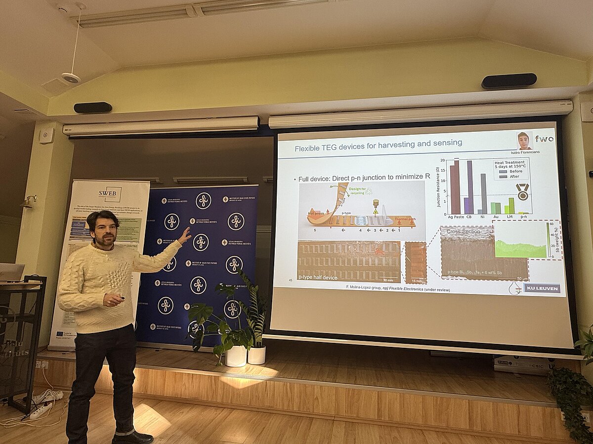
Dr. Francisco Molina-Lopez (KU Leuven, Belgium) delivered the second lecture, “Printed Flexible Thermoelectrics for Low Power Applications”, focusing on printed and flexible thermoelectric technologies capable of harvesting low-grade waste heat from curved and irregular surfaces—an attractive route for powering low-energy electronics in wearables and Internet-of-Things applications. He discussed the performance–processability trade-off that often limits printed thermoelectrics and presented approaches that combine materials insight with processing innovation and device engineering. By leveraging methods such as brush and laser printing, his work advances the deposition and patterning of thermoelectric materials on flexible substrates and supports integration into practical device architectures.
Beyond the scientific content, the seminar reflects SWEB’s wider objectives to build long-term research capacity and durable partnerships around smart energy technologies. Besides advancing smart-window-related materials and devices, project strengthen human capital, develop transferable competences (from advanced fabrication and testing to innovation and exploitation), and expand cooperation with leading European R&I organisations and industry. A core part of this approach is creating opportunities that help form new consortia and identify shared R&D agendas, so that follow-up proposals and joint projects can be prepared in line with SWEB’s mission and sustained beyond the project lifetime. Events like this seminar provide exactly that “meeting ground”: connecting complementary expertise in additive manufacturing, sustainable printed electronics, and low-power energy harvesting, while opening concrete routes for collaboration and future proposal development aligned with SWEB’s ambitions.