
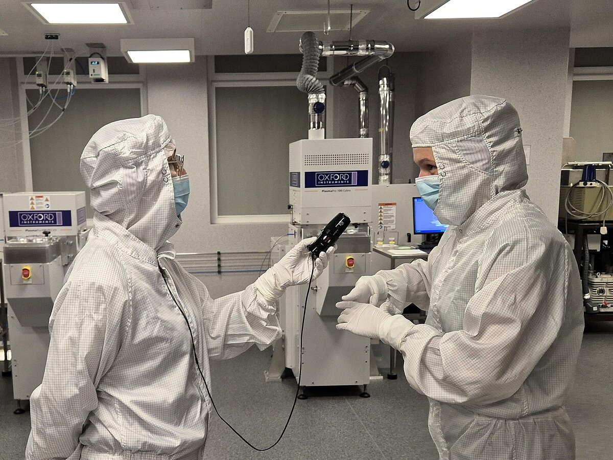
In the 18 June broadcast of the Latvian Radio programme Zināmais nezināmajā (Known in the Unknown), listeners had the opportunity to follow a tour through the Cleanrooms of the Institute of Solid State Physics, University of Latvia (ISSP UL), learning about the specifics of the its work and equipment.
The Head of the Micro and Nano Devices Laboratory, Maira Elksne, accompanied the journalists from donning the special protective suits and passing through the air shower for disinfection, to introducing the equipment used to develop components for technologies so small that an eyelash falling onto a sample could cause serious damage – hence the importance of hoods, masks, gloves, and other isolating gear.
The segment also focused on the lithography process, which is fundamental to the creation of various types of microelectronics. “We can’t cut nanometre-sized materials by hand, so we use other methods. For example, we design the required device with precise dimensions on a computer, then create a resist stencil on our sample, and use various machines to coat it evenly, harden it, and engrave it using UV light or electrons,” Maira explained in simple terms.
The full segment (in Latvian) can be heard on the platform REplay.lv (from 6:06 to 18:30)